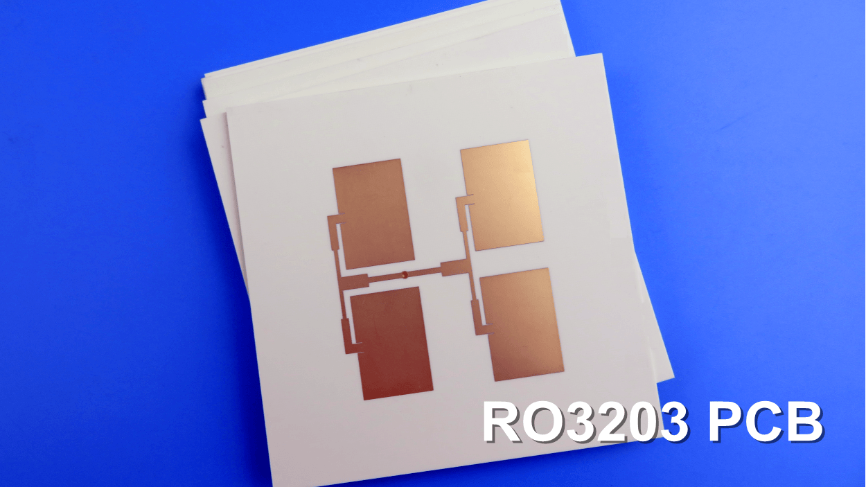
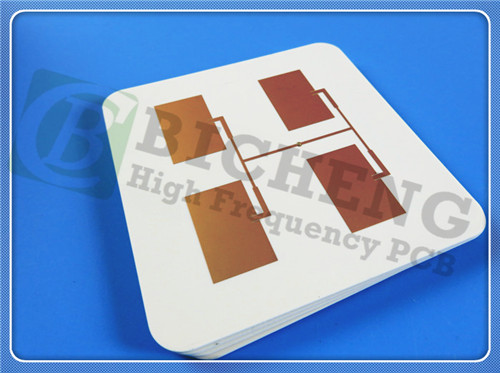
RO3203 2-Layer 10mil ENEPIG PCB for High-Frequency Wireless Systems
1. Introduction of RO3203
RO3203 High Frequency Circuit Materials are ceramic-filled laminates reinforced with woven fiberglass. These materials are engineered to offer exceptional electrical performance and mechanical stability at competitive prices. The RO3203 High Frequency Materials were designed as an extension of the RO3000 Series High Frequency Circuit Materials with one distinguishing characteristic - improved mechanical stability. The dielectric constant of RO3203 High Frequency Circuit Materials is 3.02. This, along with a dissipation factor of 0.0016, extends the useful frequency range beyond 40 GHz.
2. Key Features
Advanced Material: Rogers RO3203 ceramic-filled PTFE composites
Stable Dielectric Constant: 3.02 ±0.04 at 10 GHz/23°C
Ultra-Low Loss: Dissipation factor of 0.0016 at 10 GHz/23°C
High Temperature Resistance: Td > 500°C
Effective Thermal Management: Thermal Conductivity of 0.87 W/mK
Excellent Thermal Stability: CTE X-axis 13 ppm/°C, Y-axis 13 ppm/°C, Z-axis 58 ppm/°C (-55 to 288°C)
Modern Compliance: Lead free Process Compatible, 94V-0 flammability
3. Benefits
Enhanced Mechanical Properties: Woven glass reinforcement improves rigidity for easier handling
Consistent Performance: Uniform electrical and mechanical performance ideal for complex multi-layer high frequency structures
Superior High-Frequency Capability: Low dielectric loss enables high frequency performance in applications exceeding 20 GHz
Reliable Integration: Low in-plane expansion coefficient (matched to copper) suitable for epoxy multi-layer board hybrid designs and reliable surface mounted assemblies
Manufacturing Efficiency: Excellent dimensional stability ensures high production yields
Cost Effectiveness: Economically priced for cost effective volume manufacturing
Precision Manufacturing: Surface smoothness allows for finer line etching tolerances
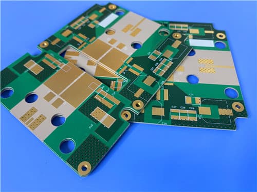
4. PCB Construction Details
| Parameter |
Specification |
| Base Material |
RO3203 |
| Layer Count |
2-Layer |
| Board Dimensions |
74.57mm × 23.28mm = 1PC |
| Minimum Trace/Space |
4/7 mils |
| Minimum Hole Size |
0.2mm |
| Blind Vias |
No |
| Finished Board Thickness |
0.35mm |
| Finished Cu Weight |
1oz (1.4 mils) outer layers |
| Via Plating Thickness |
20 μm |
| Surface Finish |
ENEPIG |
| Top Silkscreen |
White |
| Bottom Silkscreen |
No |
| Top Solder Mask |
Green |
| Bottom Solder Mask |
No |
| Electrical Test |
100% tested prior to shipment |
| Design Standard |
IPC-Class-2 |
| Artwork Format |
Gerber RS-274-X |
| Availability |
Worldwide |
5. PCB Stackup (2-Layer Rigid Structure)
Copper Layer 1 - 35 μm
Rogers RO3203 Substrate - 10mil (0.254mm)
Copper Layer 2 - 35 μm
6. PCB Statistics:
Components: 12
Total Pads: 32
Thru Hole Pads: 18
Top SMT Pads: 14
Bottom SMT Pads: 0
Vias: 33
Nets: 2
7. Typical Applications
Automotive collision avoidance systems
Automotive global positions satellite antennas
Wireless telecommunications systems
Microstrip patch antennas for wireless communications
Direct broadcast satellites
Datalink on cable systems
Remote meter readers
Power backplanes
LMDS and wireless broadband
Base station infrastructure
8. Quality Assurance
Artwork Format: Gerber RS-274-X
Accepted Standard: IPC-Class-2
Availability: Worldwide
|
.jpg)
.jpg)
.jpg)
.jpg)